Introduction
The semiconductor business' mission for better execution, lower power utilization, and cost proficiency has driven developments in electronic bundling advances. Customary bundling strategies, while compelling before, presently face impediments in scaling, warm administration, and sign respectability. High level bundling arrangements have arisen to address these difficulties, offering critical enhancements in coordinating various parts into single gadgets, improving sign associations, and streamlining in general Advanced Packaging Enables Energy-efficient Computing.
The Evolution of Electronic Packaging

Traditional Packaging Methods
Dual In-line Package (DIP):
The Plunge technique highlights two equal columns of pins for through-opening mounting on PCBs. It was generally utilized in the beginning of semiconductor gadgets because of its straightforwardness and usability. Notwithstanding, its enormous size and restricted pin count limited its versatility and execution.
Read Also: How Does Geothermal Energy Work? Step By Step Guide
Inefficient Heat Dissipation:
Warm administration is difficult for customary bundling strategies. As power thickness increments, viable intensity scattering becomes vital to keeping up with execution and dependability. Customary techniques frequently need effective intensity dissemination components, prompting overheating and execution debasement.
Signal Respectability Issues:
Higher information rates and sign frequencies in present day ICs can prompt sign uprightness issues like weakening, crosstalk, and electromagnetic impedance (EMI). Conventional bundling strategies battle to keep up with signal honesty over lengthy interconnects, influencing in general execution.
Higher Power Utilization:
Conventional bundling techniques frequently bring about a more powerful utilization because of longer interconnects and wasteful power conveyance. As gadgets become more power-delicate, diminishing power utilization turns into a basic prerequisite.
High level Bundling Innovations
Framework in-Bundle (Taste)
Framework in-Bundle (Taste) coordinates numerous ICs and latent parts into a solitary bundle, empowering more minimal and productive plans.
Decreased Structure Element: Taste innovation considers the combination of various parts like processors, memory, and sensors into a solitary bundle. This decreases the general structure component of electronic gadgets, making them more modest and Advanced Packaging Enables Energy-efficient Computing.
Further developed Execution: By coordinating different parts into a solitary bundle, Taste diminishes the interconnect length and opposition, bringing about better electrical execution. The more limited interconnects additionally improve signal honesty and lessen dormancy.
Lower Power Utilization: Taste innovation limits power misfortune by lessening the interconnect length and opposition. This prompts lower power utilization and further developed energy effectiveness, making it ideal for battery-controlled gadgets.
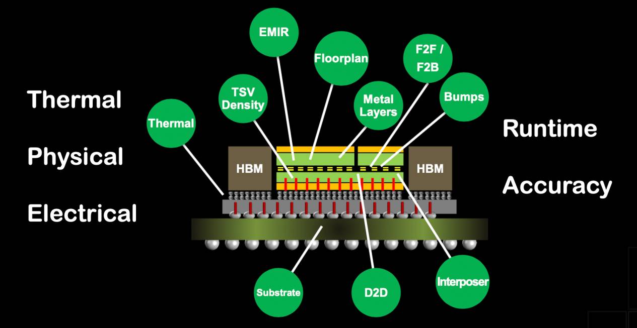
3D Bundling
3D bundling includes stacking numerous layers of ICs in an upward direction, associated through TSVs.
Wafer-Level Bundling (WLP) processes are performed at the wafer level prior to dicing, bringing about more modest and more practical bundles.
More modest Size: WLP innovation disposes of the requirement for discrete bundling steps, bringing about more modest and more slender bundles. This is great for applications that require reduced and lightweight plans, like cell phones and wearables.
Worked on Warm Execution: WLP innovation offers better warm execution contrasted with conventional bundling strategies. The nearness of the bite the dust to the bundle surface improves heat dispersal, forestalling warm prompted execution debasement.
Cost-Adequacy: WLP processes are performed at the wafer level, lessening the quantity of gathering steps and materials required. This brings down assembling costs and further develops creation proficiency, making WLP a practical answer for high-volume applications.
Fan-Out Wafer-Level Bundling (FO-WLP)
Fan-Out Wafer-Level Bundling (FO-WLP) broadens the IC impression past the bite the dust edge, considering higher I/O thickness and better warm administration.
Higher I/O Thickness: FO-WLP innovation empowers the mix of more I/O associations in a solitary bundle by expanding the IC impression past the kick the bucket edge. This builds the general I/O thickness, further developing information move rates and execution.
Better Warm Administration: FO-WLP innovation improves warm administration by giving more surface region to warm dissemination. This diminishes the gamble of overheating and works on generally speaking unwavering quality and execution.
Cost Decrease: FO-WLP innovation diminishes the expense of bundling by killing the requirement for complex interposer structures. This works on the assembling system and brings down creation costs, making FO-WLP an appealing choice for cost-delicate applications.
Must Read: Media Brief: Canada’s Clean Electricity Regulations
Through-Silicon Vias (TSVs)
Through-Silicon Vias (TSVs) are upward electrical associations going through the silicon wafer, empowering high-transfer speed correspondence between stacked ICs.
High Transmission capacity: TSVs give high-data transfer capacity correspondence between stacked ICs, empowering quicker information move and further developed execution. This is fundamental for applications that require rapid information handling, like computer based intelligence and ML.
Low Power Utilization: TSVs diminish power utilization by limiting the interconnect length and obstruction. This prompts lower power misfortune and further developed energy productivity, making TSVs reasonable for battery-fueled gadgets and applications requiring a low-influence activity.
Decreased Structure Component: TSVs empower the vertical stacking of ICs, lessening the general structure variable of electronic gadgets. This is great for applications that require minimal and lightweight plans, like cell phones and wearables.
Influence on Power Proficiency
Diminished Power Utilization
High level bundling advancements lessen power utilization by limiting interconnect lengths and opposition. More limited interconnects bring about lower power misfortune and further developed energy proficiency, making these innovations ideal for battery-fueled gadgets and applications requiring a low-influence activity.
Improved Warm Administration:
High level bundling advances offer better warm administration, decreasing the gamble of overheating and warm actuated execution debasement. Productive intensity scattering components, like TSVs and further developed heat spreaders, guarantee that intensity created during activity is really made due, keeping up with the trustworthiness and execution of the Advanced Packaging Enables Energy-efficient Computing.
Power The board Strategies
Dynamic Voltage and Recurrence Scaling (DVFS):
DVFS changes the voltage and recurrence of the processor in view of responsibility necessities, improving power utilization. High level bundling advances empower more productive DVFS by decreasing interconnect lengths and working on warm administration.
Power Gating:
Power gating separates power from latent circuits to diminish the spillage of force. High level bundling advances upgrade power gating by giving more effective and solid interconnects, decreasing power misfortune, and further developing energy proficiency.
Multi-Vt Plan:
Multi-Vt configuration uses semiconductors with various edge voltages to adjust execution and power effectiveness. High level bundling advances empower more exact and dependable multi-Vt plans, upgrading power utilization and execution.
Influence on Execution
Worked on Signal Trustworthiness
Decreased Signal Lessening and Crosstalk:
High level bundling innovations improve signal honesty by decreasing sign constriction and crosstalk. More limited interconnects and further developed electrical execution bring about higher information transmission velocities and more solid correspondence between parts, basic for superior execution figuring and correspondence frameworks.
Improved Information Transmission Velocities:
High level bundling innovations empower higher information transmission speeds by decreasing inactivity and working on signal uprightness. This is fundamental for applications, for example, 5G, man-made intelligence, and AI, where fast information handling is vital.
Higher Transmission capacity and Information Rates

Expanded I/O Thickness:
High level bundling advancements increment I/O thickness, empowering higher transmission capacity and information rates. This is especially useful for applications that require rapid information move, for example, server farms and elite execution figuring.
Diminished Dormancy:
High level bundling advances diminish inactivity by limiting interconnect lengths and working on signal respectability. This improves in general framework execution and responsiveness, fundamental for ongoing applications and superior execution processing.
Improved Warm Administration
Effective warm administration is crucial for keeping up with ideal execution and unwavering quality of coordinated circuits. High level bundling advances offer better warm scattering, forestalling warm initiated execution debasement. Methods, for example, the utilization of TSVs and further developed heat spreaders guarantee that intensity created during activity
Influence on Cost
Financially savvy Assembling
High level bundling arrangements add to financially savvy fabricating by decreasing material use and smoothing out gathering processes. By coordinating different parts into a solitary bundle, the general impression is limited, bringing about lower creation costs. Moreover, wafer-level handling methods utilized in WLP and FO-WLP improve fabricating proficiency, prompting Advanced Packaging Enables Energy-efficient Computing.
Yield Improvement
Higher assembling yields is a huge benefit of cutting edge bundling innovations. By limiting imperfections and upgrading process control, these advances further develop yield rates, diminishing the general expense per unit. Procedures, for example, TSVs and 3D bundling additionally take into consideration better use of silicon wafers, further adding to cost proficiency.
Adaptability and Adaptability
High level bundling innovations offer versatility and adaptability, making it more straightforward to incorporate heterogeneous parts and adjust to various applications and markets. This versatility decreases improvement costs and speeds up chance to-mama